
The new type of perovskite is one of the hot research materials, and its related research has made great progress in the fields of solar cells, light-emitting diodes and photodetectors. The preparation process of optoelectronic devices and electronic devices based on perovskite materials is simple, and it is easy to manufacture and integrate in a large area and be integrated into classic electronic devices. However, there are still few studies on field effect transistors based on perovskite materials. The reported work has problems such as low carrier mobility and unknown transmission mechanism.
In response to this problem, Guo Chunlei of the Changchun Institute of Optics, Fine Mechanics and Physics, Chinese Academy of Sciences, China's Yu Weili team at the Sino-U.S. Joint Photonics Laboratory, used the method of spatial confinement and inverse temperature crystallization to prepare CsPbBr3 with low defect density The thin single crystal overcomes the problem that carriers are susceptible to the influence of grain boundaries and grain defects during lateral channel transmission, and an efficient photosensitive field effect transistor is prepared.
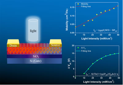
The CsPbBr3 thin single crystal grown by the method of combining space confinement and inverse temperature crystallization has no obvious grain boundary domains, the thickness is about 2 microns, and the size can reach the millimeter level or larger, which is convenient for electronic and optoelectronic devices. Preparation and application. The field effect transistor based on this thin single crystal is bipolar at room temperature, and its carrier transport exhibits a strange light intensity dependence: the mobility of electrons is independent of the intensity of light, and the mobility of holes varies with the intensity of light When the electrons are majority carriers, the threshold voltage shows light dependence, while the holes are majority carriers without this phenomenon. This is the first time this phenomenon has been reported in perovskite materials. The author analyzes that this special transmission characteristic is caused by the photoconductive effect and the photovoltaic effect, respectively, and reflects the particularity of the carrier transmission mechanism of the perovskite material. Under the illumination condition of 50 mW / cm2, the prepared field effect transistor has an electron (hole) mobility of 0.40 (0.34) cm2 V-1 s-1 at room temperature, which is significantly better than the reported based on Field effect transistor of CsPbBr3 perovskite material. In addition, the fabricated devices also exhibited excellent photodetector performance.
This work not only provides a guiding strategy for the preparation of high-performance photosensitive field-effect transistors, but also reveals the unique charge transport mechanism of all-inorganic perovskite CsPbBr3, which will help the subsequent study of the photoelectric characteristics of perovskite materials and device optimization . The related results were published in Advanced Optical Materials (DOI: 10.1002 / adom.201900676) under the title Anomalous Ambipolar Phototransistors Based on All-Inorganic CsPbBr3 Perovskite at Room Temperature.
The steel inserts are hardened with a zinc and clear chromate finish. Stainless are type 303. Can be installed with hand installation tools. Optimum hole size to be determined through experimentation. A 60 degrees countersink is required for flush mounting. For use in aluminum, aluminum alloy, magnesium and mild steel.
Carbon Steel Insert,Carbon Steel Key-Locking Thread Insert,Carbon Steel Thread Repair Insert,Heavy Duty Carbon Steel Keensert
Shenyang Helisert Technology Co., Ltd , https://www.helisert.com